The whole route is expensive
Tools, sign-off, masks, fabrication, packaging and test can push a standalone program past $1M.
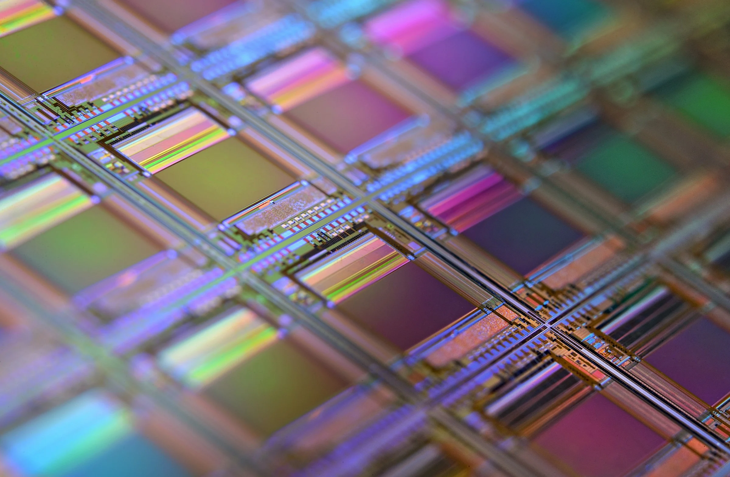
A faster path from finished design to packaged silicon. Around 6 months, at roughly one fifth of the usual cost, with no in-house chip team.
Tools, sign-off, masks, fabrication, packaging and test can push a standalone program past $1M.
Access, contracts, sign-off, shuttle timing, fabrication and packaging turn one tape-out into a long program.
Only 14% of IC/ASIC projects achieved first-silicon success in a 2024 industry study.
For qualified designs, our fast channel shares the wafer and manages the complete manufacturing route from design handoff to packaged parts.
Cost benchmarkRoughly one fifthCompared with a standalone low-volume route for a qualified design.
Fast-channel scope180 nm to 40 nmBuilt around scheduled MPW runs, available PDKs and a tape-out-ready design.
Delivered outputPackaged partsReady for bring-up, with full production test coming.
We review your GDS, target node, die size, interfaces, packaging needs and production goals to confirm the right route.
Once the route is set, we run DRC, LVS and timing checks before your design goes near a wafer.
Your design rides with others. You pay for a slot, not a full mask set.
You receive packaged parts, ready for bring-up. Full test is coming.
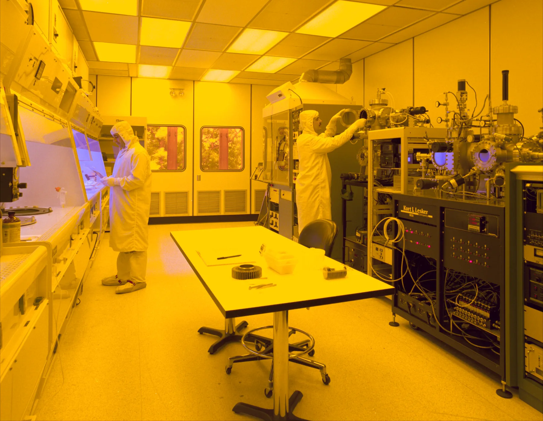
Your engineers keep building the product. Mozaic handles the manufacturing work that normally needs dedicated silicon operations.

For teams building specialized silicon on mature and mid-range nodes from 180 nm to 40 nm.
30 minute feasibility call
Bring your design stage, target node and quantity. Leave with a realistic route, cost range and next step.